NVIDIA Advances Computational Lithography Platform with TSMC and Synopsys.
TSMC and Synopsys decided to integrate NVIDIA’s cuLitho into their processes. The aim is to speed up chip manufacturing and support future GPUs. They anticipate improved efficiency and compatibility in chip production.
At the GTC Developer Conference, Huang Renxun emphasized the significance of computational lithography. He highlighted cuLitho, a collaborative effort with TSMC and Synopsys. The technology utilizes accelerated computing and AI, paving the way for semiconductor advancements.
NVIDIA introduced a new generative AI algorithm and improved cuLitho, a GPU-accelerated lithography library. This advancement offers substantial enhancements over CPU-based methods in semiconductor manufacturing.
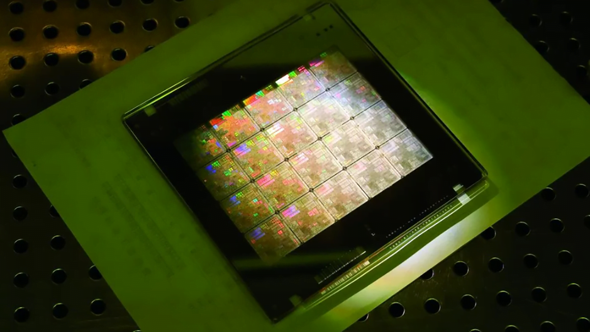
Computational lithography stands as the most demanding task in semiconductor manufacturing, devouring tens of billions of CPU hours annually. Calculating a standard mask set necessitates approximately 30 million CPU hours, prompting semiconductor foundries to construct extensive data centers.
Nvidia says that with 350 Nvidia H100 systems, they can replace 40,000 CPU systems. Additionally, this transition not only accelerates production times but also simultaneously reduces costs, space, and power consumption.
NVIDIA said that the advantages of cuLitho have already been demonstrated in TSMC’s production process. The two companies have jointly achieved a 45-fold increase in curve process speed and a nearly 60-fold increase in the traditional Manhattan process.
NVIDIA has developed algorithms that leverage generative artificial intelligence to further augment the capabilities of the cuLitho platform. On top of the accelerated processes achieved through cuLitho, the new generative AI workflow is an additional 2x faster.
By applying generative artificial intelligence, it is possible to create a near-perfect inverse mask or inverse solution that takes into account the diffraction of light. Moreover, subsequent to this transition, the final reticle is obtained through conventional rigorous physical methods. This accelerates the entire optical proximity correction (OPC) process by a factor of two.
Currently, many changes in fab processes require modifications to OPC, increasing the amount of calculations required and creating bottlenecks in the fab development cycle. The accelerated computing and generative artificial intelligence provided by cuLitho alleviates these costs and bottlenecks, allowing factories to allocate available computing power and engineering bandwidth to design more novel solutions as they develop new technologies at 2nm and beyond.

