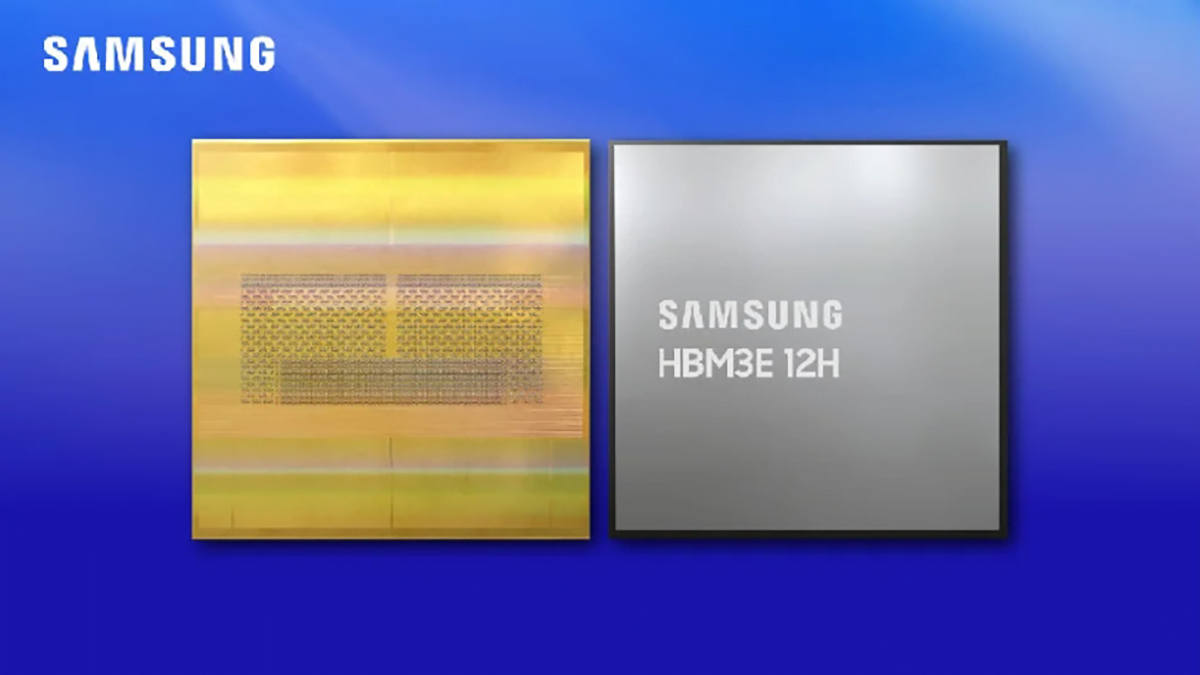
Samsung Electronics announced today the official release of its first 12 layer stacked HBM3E DRAM product – HBM3E 12H, marking a new technological breakthrough for Samsung in the HBM field.
This product is not only Samsung largest HBM product to date, but it also supports a maximum bandwidth of 1280GB/s 24/7, with a product capacity of up to 36GB DRAM.
Compared to Samsung’s 8-layer stacked HBM3 8H, HBM3E 12H has achieved over 50% improvement in bandwidth and capacity. Yongcheol Bae, Executive Vice President of Samsung’s Memory Product Planning Team, stated, “Currently, artificial intelligence service providers in the industry increasingly require higher capacity HBMs, and our new product, HBM3E 12H, is designed to meet this demand.”
The newly released HBM3E 12H adopts hot pressed non-conductive thin film (TC NCF) technology, maintaining the height consistency of 12 and 8-layer stacked products to meet the current HBM packaging requirements. This technology can not only alleviate the chip bending problem caused by thin films, but also bring more benefits in higher stacking. Samsung has committed to reducing the thickness of non-conductive thin film (NCF) materials, minimizing the gap between chips to 7 micrometers (µ m), and eliminating the gap between layers. These efforts have increased the vertical density of HBM3E 12H by more than 20% compared to HBM3 8H.
Samsung’s TC NCF technology enhances HBM’s thermal performance by enabling varied bump sizes between chips. During the chip bonding process, manufacturers use smaller protrusions for signal transmission areas and place larger protrusions in areas that require heat dissipation. This innovative method helps to improve product yield.
Samsung Electronics claims HBM3E 12H can enhance AI training speeds by 34% compared to HBM3 8H. Additionally, the number of inference service users will increase by more than 11.5 times.
Samsung now samples HBM3E 12H, aiming mass production in the year’s second half. This technological breakthrough marks Samsung’s continuous efforts and technological leadership in the core technology field of multi-layer stacked HBM.

