Challenges and Expansions in HBM Memory Production: Addressing Low Yield Amidst Growing AI Demand
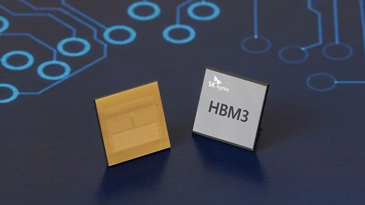
DealSite reported SK Hynix and Samsung Electronics’ plans to significantly expand HBM memory production this year. However, despite the considerable attention on HBM in the AI semiconductor market, it faces challenges like low yield, limiting its ability to meet the growing demand in the AI market.
HBM memory uses wafer-level packaging (WLP) technology, connecting multiple layers of DRAM memory wafers through TSV silicon through holes. A setback in one layer of DRAM results in discarding the entire HBM stack. For example, with 8-layer stacked products and assuming a 90% yield for each stack, the overall yield of the HBM stack drops to just 43%, with over half of the DRAM discarded. As the number of HBM layers increases, such as with the 12 or 16 layer stack, the yield further diminishes.
Currently, DealSite reports the overall yield of HBM memory at approximately 65%, significantly lower than traditional memory products. Achieving an increased yield to 80% or 90% proves challenging due to the inherent nature of WLP.

Expanding HBM Memory Production: SK Hynix and Samsung Respond to Market Demands Amid Capacity Challenges
However, SK Hynix and Samsung Electronics, leading players in the HBM memory market, are both substantially increasing their production this year. Kiwoom Securities, a South Korean securities firm, predicts Samsung Electronics’ monthly HBM memory production capacity to rise from 25,000 wafers in Q2 of last year to 15.17 million wafers in Q4 of this year. Simultaneously, SK Hynix’s monthly production capacity is expected to jump from 35,000 pieces to 12.14 million pieces. This indicates that, despite challenges, both manufacturers are actively responding to market demand and the growing semiconductor market.
Nevertheless, the capacity growth of SK Hynix and Samsung remains insufficient compared to the demand for HBM memory in the AI market. SK Hynix executives have confirmed the complete sell-out of this year’s HBM capacity quota. According to a NEWSIS report at the end of last year, Samsung has already finalized negotiations with major customers regarding this year’s production capacity.

